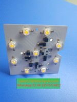
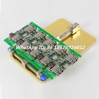
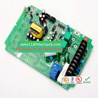
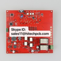
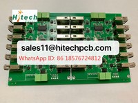
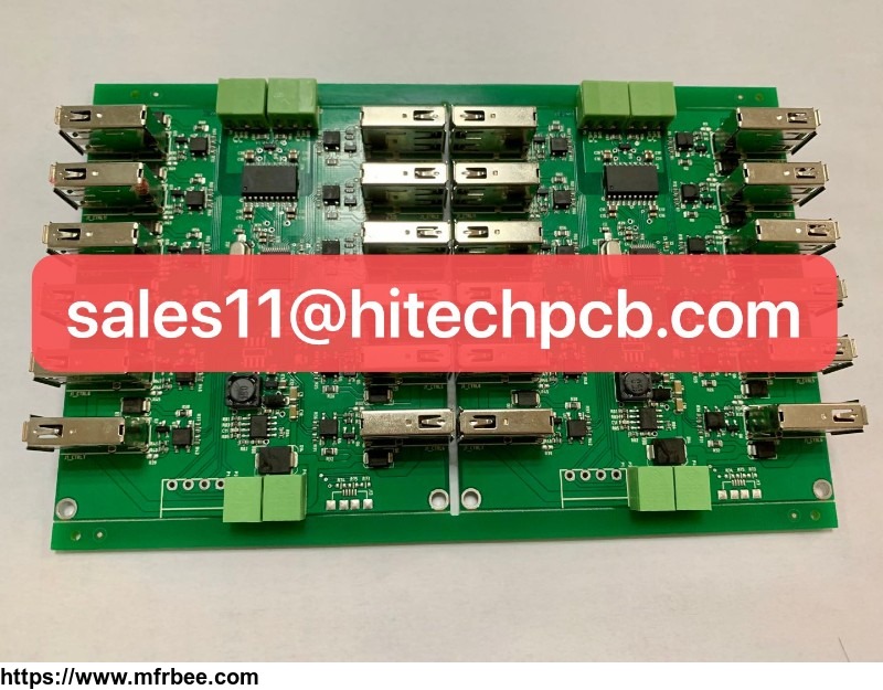
PCB Assembly and Components Sourcing
Quick Detail
- FOB Price : USD $16.00 / Piece
- Minimum order:5
- Place of Origin:China (Mainland)
Specifications
PCBA appearance inspection instructions
1,The lack of components: In the corresponding position, no solder components in accordance with the requirements.
2,dry soldering: component not tin or the tin is less than three-quarters of the solder joint area (SMT components for the solder area is less than the width of 1/2 of component).
3,continuous tin electrodeposit: due to abnormal operation, connect of two point which are disconnected on the electrical with tin.
4,Error components: the components which is soldered on board is not match with the BOM.
5,Pseudo Soldering: Component’s pin is not solder well, can not guarantee effective welding (including fake welding).
6,Cold welding: welding surface is gray, no wetting well.
7,Reverse: The polarity of the component after mounting is opposite to that specified in the document.
8,Build monument: One end of the components tilt away from the pad to form a monument.
9,Positive and negative solder wrong:The front of the assembly (silkscreen side) faces down but the soldering is normal.
10,Open circuit: Component’s pins are disconnected or the PCBA board line is disconnected.
11,Tipped: Line copper foil or pad detached from PCBA board and raised beyond specification.
12,Excess components: The file indicates the location of a component without the presence of components on the PCBA board.
13,Tin cracking: usually after the solder joint is subjected to external force, the solder joint and the component lead are separated, which has an impact on the welding effect.