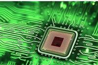
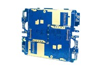
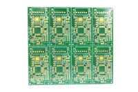
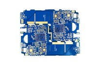
4Layer PCBA

Description
| Delivery Time: | 20 working days |
| Package: | Seal packing; we can package according to customer's request. |
| Supply Ability: | 10000 Piece/Pieces per Month |
| Minimum Order Quantity: | 10 Piece/Pieces |
| Payment Terms: | T/T,Western Union |
| Port: | Shenzhen |
| Fob Price: | US$10-100Shenzhen |
| Min. Line Width: | 0.20MM |
| Min. Hole Size: | 0.3MM |
| Board Thickness: | 1.6MM |
| Copper Thickness: | 0.5OZ |
| Base Material: | FR4 |
| Model Number: | JB017 |
| Brand Name: | JB |
| Place of Origin: | Guangdong China (Mainland) |
Product Details
Products involved fields: consume Electronics, Medical equipments, Industrial commands, communications, auto parts ect.
Min. parts footpins: 0201
Min. SMT Ptich: 12 mil (0.2 mm)
Surface Finish: Hard Gold / ENIG / HASL / Carbon Ink / OSP (ENTEK CU 106 AX) / Immersion Tin
Impedance: +/- 10%
Warpage: 0.5 %
Solder Mask: Solder Mask Bridge Between Solder Dam 3 mil (0.07 mm)
Micro Via: 4 mil (0.1 mm)
Hole to Edge Tolerance: +/- 5 mil (0.13 mm)
Hole to Hole Tolerance: +/- 3 mil (0.08 mm)
Minimum Via Size: 8 mil (0.2 mm)
Via / Drill Size: Minimum Drill Hole Diameter 10 mil (0.25 mm)
Layer to Layer Registration: +/- 5 mil (0.13 mm)
Maximum Thickness(10layers): 200 mil (5.0 mm)
Minimum Thickness (8 Layers): 24 mil (0.6 mm)
Minimum Thickness (6 Layers): 16 mil (0.4 mm)
Minimum Thickness (4 Layers): 12 mil (0.3 mm)
Minimum Thickness (2 Layers): 4 mil (0.1 mm)
Layer Count & Thickness: 2-12 layers
Minimum Line Spacing (External): 4 mil (0.1 mm) for mass production and 3 mils for samples.
Minimum Line Width (External): 4 mil (0.1 mm) for mass production and 3 mils for samples.
Minimum Line Width (Internal) 4 mil (0.1 mm) for mass production and 3mil for samples
Line Width & Spacing:
Maximum Panel Size: 26 X 26 (660mm X 660mm)
Material used: FR4, High Tg Minimum 170
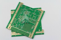
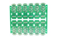
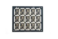
4Layer PCBA. Material FR4, PCB thickness 1.6MM, copper thickness 0.5oz, surface treatment immersion Tin.
- Solder mask:Green
- Surface Finishing:Immersion Tin
- Min. Line Spacing:0.20MM
- Min. Line Width:0.20MM
- Min. Hole Size:0.3MM
- Board Thickness:1.6MM
- Copper Thickness:0.5OZ
- Base Material:FR4
- Model Number:JB017
- Brand Name:JB
- Place of Origin:Guangdong China (Mainland)
Relate products of 4Layer PCBA

PCBA parts Assembly is a process of connecting components to a Printed Circuit Board (PCB) to form a functioning electronic device. It involves soldering components onto the board, mounting the board into an enclosure, and wiring the components together. smt pcba assembly is a ...
A pcb assembly services (PCBA) is a printed circuit board populated with electronic components. It is a finished product that is ready for use. The main difference between PCB and PCBA is that a PCB is an empty board, while a PCBA is a fully assembled board with components ...
High Speed PCB Panasonic Megtron4/6/7 TU-872SLK/Isola-FR408HR,etc Impedance Tolerance ±5%(min) Dimension Accuracy ±0.02mm(min) Line Width/Space Accuracy ±5% Founded in 2007,PEAK ...
Number of layers: 4 Surface finish: ENIG Base material: FR4 Outer Layer W/S: 6/4mil Inner layer W: 21mil Thickness: 0.4mm Min. hole diameter: 0.2mm Special process: impedance control+half hole Advantages Of 4 Layer ENIG Impedance Control Half Hole PCB Electric Circuit Board Own ...
Number of layers: 4 Surface finish: ENIG Base material: FR4 Outer Layer W/S: 6/3.5mil Inner layer W/S: 6/4mil Thickness: 0.8mm Min. hole diameter: 0.28mm Special process: impedance control+half hole Advantages Of 4 Layer ENIG Impedance Control Half Hole Fr4 PCB Own lamination ...
Number of layers: 4 Surface finish: ENIG Base material: High TG FR4 Outer Layer W/S: 4/3.5mil Inner layer W/S: 4/3.5mil Thickness: 1.0mm Min. hole diameter: 0.25mm Special process: Impedance Control Advantages Of 4 Layer High TG Impedance Control Fine Pitch PCB Own lamination ...
Number of layers: 4 size:80*88mm Surface finish: ENIG Base material: Rogers FR4 4350B Min. hole diameter: 0.3mm Minimum Line Width:0.230mm Minimum Line Space:0.170mm Thickness: 1.0mm Advantages Of 4 Layer Rogers FR4 PCB Own lamination process to convenient production for ...
Number of layers: 4 Surface finish: ENIG Base material: High TG FR4 Outer Layer W/S: 4/3.5mil Inner layer W/S: 4/3.5mil Thickness: 1.0mm Min. hole diameter: 0.25mm Special process: Impedance Control Advantages Of 4 Layer High TG Impedance Control Fine Pitch PCB Own lamination ...

Number of layers: rogers fr4 size:80*88mm Surface finish: ENIG Base material: FR4+Rogers 4350B Min. hole diameter: 0.3mm Minimum Line Width:0.230mm Minimum Line Space:0.170mm Thickness: 1.0mm Advantages Of 4 Layer rogers fr4 pcb Own lamination process to convenient ...

PCB PCBA Definition Asone of professionalPCBfabrication suppliers Application of Electronics PCBA PCBA electronics Process of manufacturingPCBA board The manufacturing of the PCBA board is divided into two parts. One part is the manufacturing of the PCB itself. The other part ...