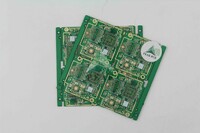
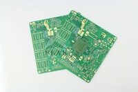
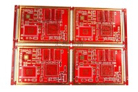
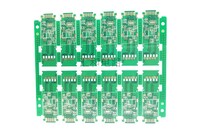
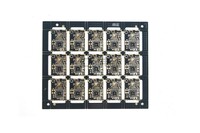
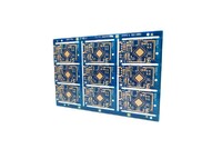
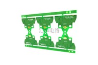
1 layer PCB

Description
| Delivery Time: | 5 days for samples and 10 days for big orders |
| Package: | Inner: VacuumOuter: Carton |
| Supply Ability: | 20000 Square Meter per Month |
| Minimum Order Quantity: | 5 Piece/Pieces |
| Payment Terms: | L/C,T/T,Western Union |
| Port: | Shenzhen |
| Fob Price: | US$0.1-15Shenzhen |
| Min. Line Spacing: | 4mil |
| Min. Line Width: | 4mil |
| Min. Hole Size: | 0.15mm |
| Board Thickness: | 1.0mm |
| Copper Thickness: | 1oz |
| Base Material: | FR1 |
| Brand Name: | ZBX |
| Place of Origin: | Guangdong China (Mainland) |
Product Details
Welcome to your detailed enquiry
Small orders can be accepted
Zhiboxin printed circuit board company is a PCB manufacturer in Shenzhen for 12 years experience, we have great advantage in multilayer PCB manufacturing, especially for two and four layers pcb board
12 years experience in China
Superior quality and competitive price
Aluminum based pcb board, double Face Gilt Panel Half Round
Multilayer PCB board
Prompt Delivery and competitive price
Quality Approval
Small Orders Accepted
- Surface Finishing:HASL
- Min. Line Spacing:4mil
- Min. Line Width:4mil
- Min. Hole Size:0.15mm
- Board Thickness:1.0mm
- Copper Thickness:1oz
- Base Material:FR1
- Brand Name:ZBX
- Place of Origin:Guangdong China (Mainland)
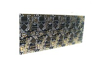
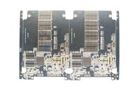
You may also like
Relate products of 1 layer PCB
Multilayer PCB Up to 64 Layers; FR4 TG135/TG150/TG170; Halogen Free/CTI≥600; Aspect Ratio (Finish Hole) 28:1; Sample Expedited 8 Hours(1-2Layer); HDI PCB Blind/Buried/Hybrid Via; 5+N(N+M)+5 Structure; Trace Width/Spacing 1.6/1.6mil; Laser Hole Size(mm)≥0.075; High Density ...
Number of layers: 8 Surface finish: ENIG Base material: FR4 Outer Layer W/S: 4/3mil Inner layer W/S: 4/3mil Thickness: 1.2mm Min. hole diameter: 0.2mm Special process: impedance control Advantages Of 8 Layer PCB Own lamination process to convenient production for Multilayer PCB ...
HDI PCB Blind/Buried Via 5+N(N+M)+5 Structure Trace Width/Spacing 1.6/1.6mil Laser Hole Size(mm)≥0.075 High Density Interconnector Founded in 2007,PEAK ...

Previous image Next image Number of layers: 16 Surface finish: ENIG Base material: FR4 Thickness: 3.0mm Min. hole diameter:0.35mm size:420×560mm Outer Layer W/S: 4/3mil Inner layer W/S: 5/4mil Aspect Ratio: 9:1 Special process: via-in-pad Impedance Control Press Fit Hole ...
Previous image Next image Number of layers: 10 Surface finish: ENIG Aspect Ratio: 8:1 Base material: FR4 Outer Layer W/S: 4/4mil Inner layer W/S: 5/3.5mil Thickness: 2.0mm Min. hole diameter:0.25mm Special process: Impedance Control, Resin Plugging, Different Copper Thickness ...
Number of layers: 8 Surface finish: ENIG Base material: FR4 Outer Layer W/S: 4/3mil Inner layer W/S: 5/4mil Thickness: 1.6mm Min. hole diameter: 0.2mm Special process: half hole Advantages Of 8 Layer ENIG Half Hole Custom Made PCB Own lamination process to convenient production ...
Number of layers: 4 Surface finish: ENIG Base material: FR4 Outer Layer W/S: 6/4mil Inner layer W: 21mil Thickness: 0.4mm Min. hole diameter: 0.2mm Special process: impedance control+half hole Advantages Of 4 Layer ENIG Impedance Control Half Hole PCB Electric Circuit Board Own ...
Number of layers: 4 Surface finish: ENIG Base material: FR4 Outer Layer W/S: 6/3.5mil Inner layer W/S: 6/4mil Thickness: 0.8mm Min. hole diameter: 0.28mm Special process: impedance control+half hole Advantages Of 4 Layer ENIG Impedance Control Half Hole Fr4 PCB Own lamination ...
Number of layers: 2 Surface finish: OSP Base material: FR4 Outer Layer W/S: 6/4mil Thickness: 1.0mm Min. hole diameter: 0.25mm Special process: impedance control+half hole Advantages Of 2 Layer OSP Impedance Control Half Hole PCB Own lamination process to convenient production ...
Number of layers: 2 Surface finish: ENIG Base material: FR4 Outer Layer W/S: 7/4mil Thickness: 1.0mm Min. hole diameter: 0.3mm Special process: impedance control+half hole Advantages Of 2 Layer ENIG Impedance Control Half Hole PCB Product Own lamination process to convenient ...