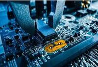
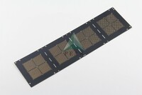
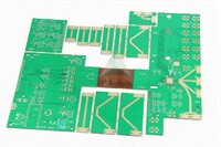
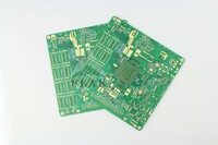
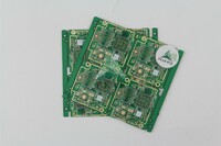
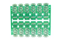
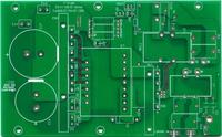
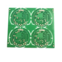
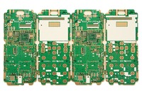
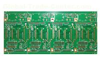
pcb board,pcb design,printed circuit board

Description
| Delivery Time: | sample within one day after payment |
| Package: | vacuum |
| Supply Ability: | 30000 Square Meter per Month |
| Minimum Order Quantity: | 5 Piece/Pieces sample |
| Payment Terms: | T/T,Western Union,MoneyGram |
| Port: | shenzhen |
| Fob Price: | US$0.1-100shenzhen |
| Min. Line Spacing: | 10mil |
| Min. Line Width: | 10mil |
| Min. Hole Size: | 0.2mm |
| Board Thickness: | 1.6mm |
| Copper Thickness: | 1OZ |
| Base Material: | FR4 |
| Brand Name: | SF |
| Place of Origin: | Guangdong China (Mainland) |
Product Details
IPC-A-600F,IPC-ML-950
IPC-A-600F,IPC-ML-950
Quality standard
OSP, HAL,Immersion GoldGold PlatingGoldfinger
OSP, HAL,Immersion GoldGold PlatingGoldfinger
Surface finish
288 10 secs
288 10 secs
Thermal shock ability
245 5 secs
245 5 secs
Solderability test
6H
6H
Soldermask hardness
0.10mm
0.10mm
Green Solder Mask Bridge
1).pcb design,pcb board manufacture
2).high quality&factory price&fast delivery&good service
3).layers:2-24
4).certificate
- Surface Finishing:OSP
- Min. Line Spacing:10mil
- Min. Line Width:10mil
- Min. Hole Size:0.2mm
- Board Thickness:1.6mm
- Copper Thickness:1OZ
- Base Material:FR4
- Brand Name:SF
- Place of Origin:Guangdong China (Mainland)
You may also like
Relate products of pcb board,pcb design,printed circuit board
Welcome to the world of Printed Circuit Board (PCB) technology from the GOLDEN TRIANGLE GROUP, one of the most professional printed circuit board China suppliers. PCB technology is an essential component of the ever-changing electronics industry. It is the foundation for modern ...
IC Substrate&Substrate-Like PCB CSP/FC-CSP/SIP/FC-BGA/WB-CSP FR4/BT/High-Speed Material Trace Width/Space 12/12μm SM Registration:±20μm Strict SM Flatness Control ≤5μm Founded in 2007,PEAK ...
Rigid-Flex PCB 2-24 Layers Book/Air-gap/Fly-tail Unsymmetrical/Semi-Flex Width of Flexible Zone 3mm(min) Dimension Accuracy ±0.05mm(min) Founded in 2007,PEAK ...
HDI PCB Blind/Buried Via 5+N(N+M)+5 Structure Trace Width/Spacing 1.6/1.6mil Laser Hole Size(mm)≥0.075 High Density Interconnector Founded in 2007,PEAK ...
Regular PCB Up to 64 Layers FR4 TG135/TG150/TG170 Halogen Free/CTI≥600 Aspect Ratio (Finish Hole) 28:1 Sample Expedited 8 Hours(1-2Layer) Founded in 2007,PEAK ...
Number of layers: 4 Surface finish: ENIG Base material: FR4 Outer Layer W/S: 6/4mil Inner layer W: 21mil Thickness: 0.4mm Min. hole diameter: 0.2mm Special process: impedance control+half hole Advantages Of 4 Layer ENIG Impedance Control Half Hole PCB Electric Circuit Board Own ...
Our Production Capability for PCB Number of Layer: 1 - 20 Layer Maximum Processing Area: 680 × 1000MM Min Board Thickness: 2 Layer - 0.3MM ( 12 mil ) 4 Layer - 0.4MM ( 16 mil ) 6 Layer - 0.8MM ( 32 mil ) 8 Layer - 1.0MM ( 40 mil) 10 Layer - 1.1MM ( 44 mil ) 12 Layer - 1.3MM ( ...
Yheng Circuit Board Electronic Co., Ltd / pcboardfactory@sina.com
Multilayer PCB Circuit Board for Wireless Router Details Product Name: Wireless Router Circuit Board Material of Board: FR-4 Number of Laye: PCB multilayer board Min.Hole Size: 5 Mil Solder Mask Color: Green Minimum Line Width and Line Moment: 0.2mm * 0.15mm Surface Treatment: ...
Yheng Circuit Board Electronic Co., Ltd / pcboardfactory@sina.com
Product Details/pcboardfactory@sina.com Product Name: Mobile Phone Circuit Board Material of Board: FR-4 Fiberglass Board Number of Laye: Double Sided PCB Min. Hole Size: 3 Mil Mobile Phone PCB Solder Mask Color: Green Min Line Width and Line moment: 0.25mm * 0.35mm Surface ...
Yheng Circuit Board Electronic Co., Ltd / pcboardfactory@sina.com
PCB Board for Encoder, Encoder Circuit Board Details: Number of laye: Four Laye PCB Material of Board: FR-4 Rigid Board Technology: Gold Immeion Product Size: 38.6mm * 18.2mm Solder Mask: Green Ink, White characte Welcome enquiries, we can customize kinds of PCB Boards, send ...
Yheng Circuit Board Electronic Co., Ltd / pcboardfactory@sina.com