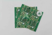
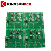
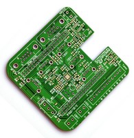
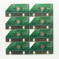
immersion Gold PCB

Description
| Delivery Time: | 20working days |
| Package: | Seal packing; we can package according to customer's request.Inner packing:vacuum packing /plastic bagOuter packing:standard carton packing |
| Supply Ability: | 50000 Piece/Pieces per Month |
| Minimum Order Quantity: | 10 Piece/Pieces |
| Payment Terms: | T/T,Western Union |
| Port: | shenzhen |
| Fob Price: | US$10-50shenzhen |
| Min. Line Width: | 0.15MM |
| Min. Hole Size: | 0.3MM |
| Board Thickness: | 1.6MM |
| Copper Thickness: | 0.5OZ |
| Base Material: | FR4 |
| Model Number: | JB009 |
| Brand Name: | JB |
| Place of Origin: | Guangdong China (Mainland) |
Product Details
Products involved fields: consume Electronics, Medical equipments, Industrial commands, communications, auto parts ect.
Min. parts footpins: 0201
Min. SMT Ptich: 12 mil (0.2 mm)
Surface Finish: Hard Gold / ENIG / HASL / Carbon Ink / OSP (ENTEK CU 106 AX) / Immersion Tin
Impedance: +/- 10%
Warpage: 0.5 %
Solder Mask: Solder Mask Bridge Between Solder Dam 3 mil (0.07 mm)
Micro Via: 4 mil (0.1 mm)
Hole to Edge Tolerance: +/- 5 mil (0.13 mm)
Hole to Hole Tolerance: +/- 3 mil (0.08 mm)
Minimum Via Size: 8 mil (0.2 mm)
Via / Drill Size: Minimum Drill Hole Diameter 10 mil (0.25 mm)
Layer to Layer Registration: +/- 5 mil (0.13 mm)
Maximum Thickness(10layers): 200 mil (5.0 mm)
Minimum Thickness (8 Layers): 24 mil (0.6 mm)
Minimum Thickness (6 Layers): 16 mil (0.4 mm)
Minimum Thickness (4 Layers): 12 mil (0.3 mm)
Minimum Thickness (2 Layers): 4 mil (0.1 mm)
Layer Count & Thickness: 2-12 layers
Minimum Line Spacing (External): 4 mil (0.1 mm) for mass production and 3 mils for samples.
Minimum Line Width (External): 4 mil (0.1 mm) for mass production and 3 mils for samples.
Minimum Line Width (Internal) 4 mil (0.1 mm) for mass production and 3mil for samples
Line Width & Spacing:
Maximum Panel Size: 26 X 26 (660mm X 660mm)
Material used: FR4, High Tg Minimum 170
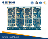
PCB Thickness 1.6mm. PCB size 180*200mm, min space/ trace 0.15mm, min holes 0.3mm, surface treatment immersion Gold.
- Solder Mask:Green
- Surface Finishing:immersion Gold
- Min. Line Spacing:0.15MM
- Min. Line Width:0.15MM
- Min. Hole Size:0.3MM
- Board Thickness:1.6MM
- Copper Thickness:0.5OZ
- Base Material:FR4
- Model Number:JB009
- Brand Name:JB
- Place of Origin:Guangdong China (Mainland)
You may also like
Relate products of immersion Gold PCB
Multilayer PCB Up to 64 Layers; FR4 TG135/TG150/TG170; Halogen Free/CTI≥600; Aspect Ratio (Finish Hole) 28:1; Sample Expedited 8 Hours(1-2Layer); HDI PCB Blind/Buried/Hybrid Via; 5+N(N+M)+5 Structure; Trace Width/Spacing 1.6/1.6mil; Laser Hole Size(mm)≥0.075; High Density ...

4L, Tg170, 0.062\", 15up, Cu: Ext: 1oz finish & Inner: 0.5oz, S/M: Green ; S/L: White, Immersion Gold: 2u\", blind routing ***Contact Information*** Email: sales@glocom.com.tw Web: www.glocom.com.tw Youtube: https://www.youtube.com/watch?v=xDIJCEdm-kU ...
Welcome to RuoMei – one of the leading manufacturers and suppliers of PCB products in China. Our factory is engaged in PCB manufacturing and offering customized rigid 10 layers gold fingers Au32u” pcb substrate fr4 with 1.6mm board thickness ENIG at competitive price. High ...
China,High quality, competitive, PCB design,manufacturer, fast delivery 12H-72H,material:94V0,CEM-1,FR4,FPC,Rigid+FPC,Aluminium,Copper,Ceramic,RogersTg170,Single,Double,Multilyer,from1 to 30L, Copper thickness:H-50 oz, HDI,Control resistant,Blind vias/Burried vias,Lead-Free ...
China,High quality, competitive, PCB design,manufacturer, fast delivery 12H-72H,material:94V0,CEM-1,FR4,FPC,Rigid+FPC,Aluminium,Copper,Ceramic,RogersTg170,Single,Double,Multilyer,from1 to 30L, Copper thickness:H-50 oz, HDI,Control resistant,Blind vias/Burried vias,Lead-Free ...
About King Sun PCB King Sun PCB Technology is a manufacturing enterprise that be engaged in high density interconnector multilayer,various types PCB prototype,small and mass production PCB produce. Our products included: HDI PCBs In 2005,we expanded our products to develop and ...
About King Sun PCB King Sun PCB Technology is a manufacturing enterprise that be engaged in high density interconnector multilayer,various types PCB prototype,small and mass production PCB produce. Our products included: HDI PCBs In 2005,we expanded our products to develop and ...
Part Number:XWS-44 Layer: 2 Layer Material: FR-4 Thickness: 1.6 MM Cooper: 2OZ Surface: ENIG (PS:With over 12 years of experience, XWS is one of worldwide leadingmanufacturer ofPCB prototyping, low volume high mix to high volume .Founded in 2006 with 200employees ...
ALLPCB Chamfer Gold Finger Contact PCB Product Prototype and Big Quantity Supported Circuit Board Shenzhen Supplier Item specifics Brand Name:ALLPCB ( www.allpcb.com/g4) Surface Finishing:ENIG Base Material:FR4 Min. Line Width:7MIL Min. Line Spacing:7MIL Min. Hole Size:0.3MM ...
14Layer HDI PCB with BGA, 2.4mm board thickness, blue solermask, surface finished by Immersion Gold 1. PCB P/N:389612 2. Layer:14L 3. Material: FR-4 4. Board thk:2.4mm 5. copper thk:35UM 6. Smallest hole size:0.15MM 7. No. of holes (pcs):1994 8. line w/s: 3/3mil 9. Impedance ...