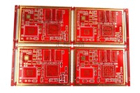
8 layer PCB(Printed Circuit Board) with blind holes

Description
| Minimum Order Quantity: | 2 Piece/Pieces |
| Payment Terms: | T/T |
| Port: | FOB Shen Zhen |
| Fob Price: | US$10-100FOB Shen Zhen |
| Min. Line Width: | 4mil |
| Min. Hole Size: | 0.3mm |
| Board Thickness: | 2.0mm |
| Copper Thickness: | 1 OZ |
| Base Material: | FR-4 |
| Model Number: | J34655M8A |
| Brand Name: | JX |
| Place of Origin: | Guangdong China (Mainland) |
Product Details
PCB(Printed Circuit Board), short lead time
PN:J34655M8A
layer count:8
distance from hole to trace:8MIL
min hole:0.3MM
min trace width/gap:4/4.3mil
aspect ratio:7:1
board thickness:2.0MM+/-0.20MM
finished treatment:blind hole+ENIG+impedance
board size:350*99.6MM
difficult point:
L1-L3 blind hole,2 times pressing, hard to control warp and twist
blind hole from L1-3
ENIG
impedance control
min hole 0.2mm
PCB(Printed Circuit Board) short lead time
- Surface Finishing:ENIG+impedance
- Min. Line Spacing:4.3mil
- Min. Line Width:4mil
- Min. Hole Size:0.3mm
- Board Thickness:2.0mm
- Copper Thickness:1 OZ
- Base Material:FR-4
- Model Number:J34655M8A
- Brand Name:JX
- Place of Origin:Guangdong China (Mainland)
You may also like
Relate products of 8 layer PCB(Printed Circuit Board) with blind holes
Number of layers: 8 Surface finish: ENIG Base material: FR4 Outer Layer W/S: 4/3mil Inner layer W/S: 5/4mil Thickness: 1.6mm Min. hole diameter: 0.2mm Special process: half hole Advantages Of 8 Layer ENIG Half Hole Custom Made PCB Own lamination process to convenient production ...
Number of layers: 4 Surface finish: ENIG Base material: FR4 Outer Layer W/S: 6/4mil Inner layer W: 21mil Thickness: 0.4mm Min. hole diameter: 0.2mm Special process: impedance control+half hole Advantages Of 4 Layer ENIG Impedance Control Half Hole PCB Electric Circuit Board Own ...

Number of layers: 8 Surface finish: ENIG Base material: FR4 Outer Layer W/S: 4/3.5mil Inner layer W/S: 4/3.5mil Thickness: 1.2mm Min. hole diameter: 0.2mm Special process: impedance control+half hole Advantages Of 8 Layer ENIG Impedance Control Half Hole PCB Own lamination ...
8 layers , Material: FR4 TG175 ,Board Thickness:0.062\" 0.5OZ base copper , trace and spacing: 3/3 mil , Blind via.min. hole:6mil ,Green soldermask, white silkscreen , impedance control , Hasl lead free , quickturn time:3WDs . Fast turn pcb has over 10 years experience on ...
Gold Multi-layer Printed Circuits Board (PCB) with aspect ratio 8:1 for industrial Solution Printed Circuits Board,Multi-layer Printed Circuits Board,Immerision Gold multi-layer Printed Circuits Board,Printed Circuits Board with aspect ratio 8:1,Printed Circuits Board for ...

Certificates: ISO 9001, ISO 14000, QS 9000, UL,... Number of Layers:8-Layer Place of Origin:Taiwan 8 Layer HDI PCB Board Prototype, FR-405 material 1.) 0.5oz Copper Foil 2.) 1.0mm Thickness 3.) Au/Ni Finished ...

Surface Finishing:ENIG+impedance control Min. Line Spacing:4mil Min. Line Width:3.5mil Min. Hole Size:0.20mm Board Thickness:2.5mm Copper Thickness:1 OZ Base Material:FR-4 Model Number:J31583M20A Brand Name:JX Place of Origin:Guangdong China (Mainland) min hole0.20mm min trace ...

Surface Finishing:ENIG+gold fingers+impedance Min. Line Spacing:5mil Min. Line Width:4.25mil Min. Hole Size:0.25mm Board Thickness:1.58mm Copper Thickness:1 OZ Base Material:FR-4 Model Number:J34595M12A Brand Name:JX Place of Origin:Guangdong China (Mainland) blind hole from ...

Surface Finishing:HAL Min. Line Spacing:5mil Min. Line Width:5mil Min. Hole Size:0.2mm Board Thickness:2.0mm Copper Thickness:1 OZ Base Material:FR-4 Model Number:J32842M8A Brand Name:JX Place of Origin:Guangdong China (Mainland) HAL+black solder mask aspect ratio:10:1 min ...

Surface Finishing:ENIG+impedance control Min. Line Spacing:5mil Min. Line Width:6mil Min. Hole Size:0.2mm Board Thickness:1.6mm Copper Thickness:1 OZ Base Material:FR-4 Model Number:J33088M10A Brand Name:JX Place of Origin:Guangdong China (Mainland) used in military products 2 ...