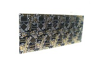
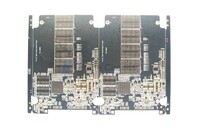
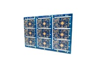
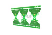
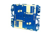
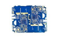
16 layer PCB(Printed Circuit Board),impedance control

Description
| Minimum Order Quantity: | 2 Piece/Pieces |
| Payment Terms: | T/T |
| Port: | FOB Shen Zhen |
| Fob Price: | US$10-100FOB Shen Zhen |
| Min. Line Width: | 6mil |
| Min. Hole Size: | 0.25mm |
| Board Thickness: | 2.0mm |
| Copper Thickness: | 1 OZ |
| Base Material: | FR-4 |
| Model Number: | J36705m16A |
| Brand Name: | JX |
| Place of Origin: | Guangdong China (Mainland) |
Product Details
Material:FR-4, Rogers, Taconic, Arlon,
Max copper:7 0Z
Max thickness:7.0mm
Finished:Leaded/Lead free HAL/OSP/ENIG/immersion Tin/immersion Silver/Hard Gold
Min trace width/gap:3/3mil
Min hole:6mil(mechanical)/4mil(laser)
Max board size:600x800mm
Aspect rati0:16:1
HDI board with 3 times pressing and 2 tims laser drill
Impedance control board.
Layer count:1-30 layer
Capability of JX PCB(Printed Circuit Board)
PN:J36705m16A
layer count:16
distance from hole to trace:10.0miL
min hole:0.25mm
min trace width/gap:6/5.4miL
aspect ratio:8:1
board thickness:2.0mm +/-0.1mm
finished treatment:HAL+green oil
board size:304*298.5mm
layer count up to 16
impedance control
HAL lead free
PCB(Printed Circuit Board)with short lead time
- Surface Finishing:HAL lead free
- Min. Line Spacing:5.4mil
- Min. Line Width:6mil
- Min. Hole Size:0.25mm
- Board Thickness:2.0mm
- Copper Thickness:1 OZ
- Base Material:FR-4
- Model Number:J36705m16A
- Brand Name:JX
- Place of Origin:Guangdong China (Mainland)
You may also like
Relate products of 16 layer PCB(Printed Circuit Board),impedance control
Number of layers: 8 Surface finish: ENIG Base material: FR4 Outer Layer W/S: 4/3mil Inner layer W/S: 4/3mil Thickness: 1.2mm Min. hole diameter: 0.2mm Special process: impedance control Advantages Of 8 Layer PCB Own lamination process to convenient production for Multilayer PCB ...
Previous image Next image Number of layers: 10 Surface finish: ENIG Aspect Ratio: 8:1 Base material: FR4 Outer Layer W/S: 4/4mil Inner layer W/S: 5/3.5mil Thickness: 2.0mm Min. hole diameter:0.25mm Special process: Impedance Control, Resin Plugging, Different Copper Thickness ...
Number of layers: 4 Surface finish: ENIG Base material: FR4 Outer Layer W/S: 6/4mil Inner layer W: 21mil Thickness: 0.4mm Min. hole diameter: 0.2mm Special process: impedance control+half hole Advantages Of 4 Layer ENIG Impedance Control Half Hole PCB Electric Circuit Board Own ...
Number of layers: 4 Surface finish: ENIG Base material: FR4 Outer Layer W/S: 6/3.5mil Inner layer W/S: 6/4mil Thickness: 0.8mm Min. hole diameter: 0.28mm Special process: impedance control+half hole Advantages Of 4 Layer ENIG Impedance Control Half Hole Fr4 PCB Own lamination ...
Number of layers: 2 Surface finish: OSP Base material: FR4 Outer Layer W/S: 6/4mil Thickness: 1.0mm Min. hole diameter: 0.25mm Special process: impedance control+half hole Advantages Of 2 Layer OSP Impedance Control Half Hole PCB Own lamination process to convenient production ...
Number of layers: 2 Surface finish: ENIG Base material: FR4 Outer Layer W/S: 7/4mil Thickness: 1.0mm Min. hole diameter: 0.3mm Special process: impedance control+half hole Advantages Of 2 Layer ENIG Impedance Control Half Hole PCB Product Own lamination process to convenient ...
Number of layers: 4 Surface finish: ENIG Base material: High TG FR4 Outer Layer W/S: 4/3.5mil Inner layer W/S: 4/3.5mil Thickness: 1.0mm Min. hole diameter: 0.25mm Special process: Impedance Control Advantages Of 4 Layer High TG Impedance Control Fine Pitch PCB Own lamination ...
Number of layers: 4 Surface finish: ENIG Base material: High TG FR4 Outer Layer W/S: 4/3.5mil Inner layer W/S: 4/3.5mil Thickness: 1.0mm Min. hole diameter: 0.25mm Special process: Impedance Control Advantages Of 4 Layer High TG Impedance Control Fine Pitch PCB Own lamination ...

Number of layers: 10 Surface finish: ENIG Aspect Ratio: 8:1 Base material: FR4 Outer Layer W/S: 4/4mil Inner layer W/S: 5/3.5mil Thickness: 2.0mm Min. hole diameter:0.25mm Special process: Impedance Control, Resin Plugging, Different Copper Thickness Advantages Of 10 Layer ...

Number of layers: 8 Surface finish: ENIG Base material: FR4 Outer Layer W/S: 4/3.5mil Inner layer W/S: 4/3.5mil Thickness: 1.2mm Min. hole diameter: 0.2mm Special process: impedance control+half hole Advantages Of 8 Layer ENIG Impedance Control Half Hole PCB Own lamination ...